The revolution in radio? RF-ARM-FPGA SoC
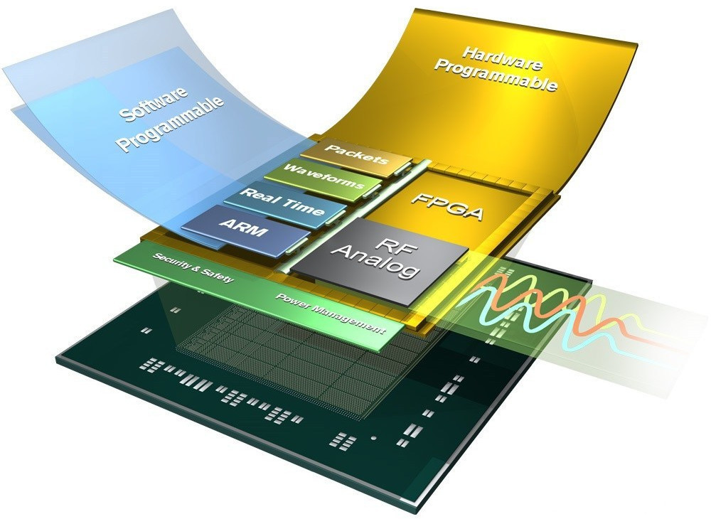
Company Xilinx quietly and without fanfare announced a product that can completely change the appearance and the development of modern radio receivers and transmitters. It's a small chip, which combines 90% treatment and formation of radio signals:
the
-
the
- programmable logic (FPGA)
the - processors for signal processing and user applications (two ARM a)
the - up to eight 12-bit ADC with sampling frequency up to 4 GHz (!),
the - up to eight 14-bit DAC with top frequencies up to 6.4 GHz (!).
It seems we are in an era where the architecture of the transceiver becomes the same versatile architecture of the modern PC. Make SW, not HW!
the
the Era before Zynq'
A bit of history. I represent a small team, the main activity of which during the last 10-15 years is R&D in the field of satellite navigation.
What we do during this time! Developed new signals for GLONASS, was treated with all possible signals, simulated signals from a navigation system, system for detection of omegapointil, were making circuits for antenna arrays, did receivers the size of a television for quantum-optical stations. In General, our adventure is safely possible to write the Kama Sutra signal processing (which we made)!
It is understandable that the zoo task we can not do the standard receivers. We love and know the modules of GEOS and NV-08C, even participated in these projects, but for our projects, we always used our own design.
The only way to do small — scale receiver based on FPGA (FPGA). It is worth to clarify that the processing modern signal resembles the work of computer graphics. The operation is relatively simple, but they need to do a lot in parallel. In this sense, the FPGA (or a piece of silicon in larger series) for the receiver as the GPU for a modern computer.
What looked like the block diagram of the receiver so ten years ago?
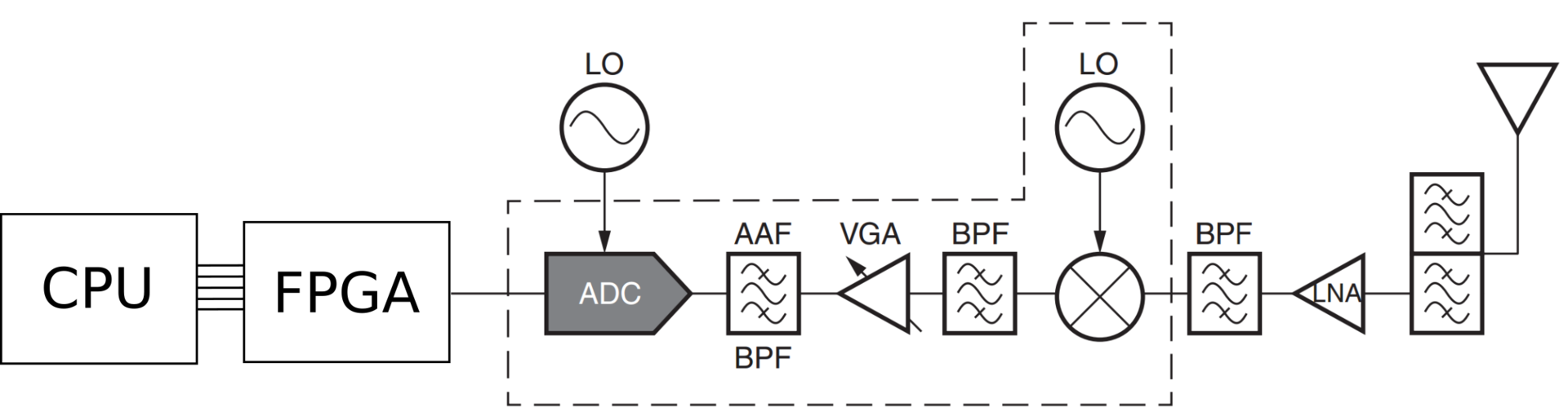
What's wrong with this scheme? Processor and programmable logic separated into different chips. And this creates a lot of problems.
The specificity of the signal processing requires a constant exchange of data between the processor and FPGA in strict real time! Flows for navigation receiver of up to several gigabits.
Each chip requires its own piping, cooling, multi-layer boards for connections and banal takes place on the PCB.
And in the end, it's just difficult. But the complexity in building systems is almost synonymous with failure.
For example, the block diagram of the receiver, which we did in 2007:
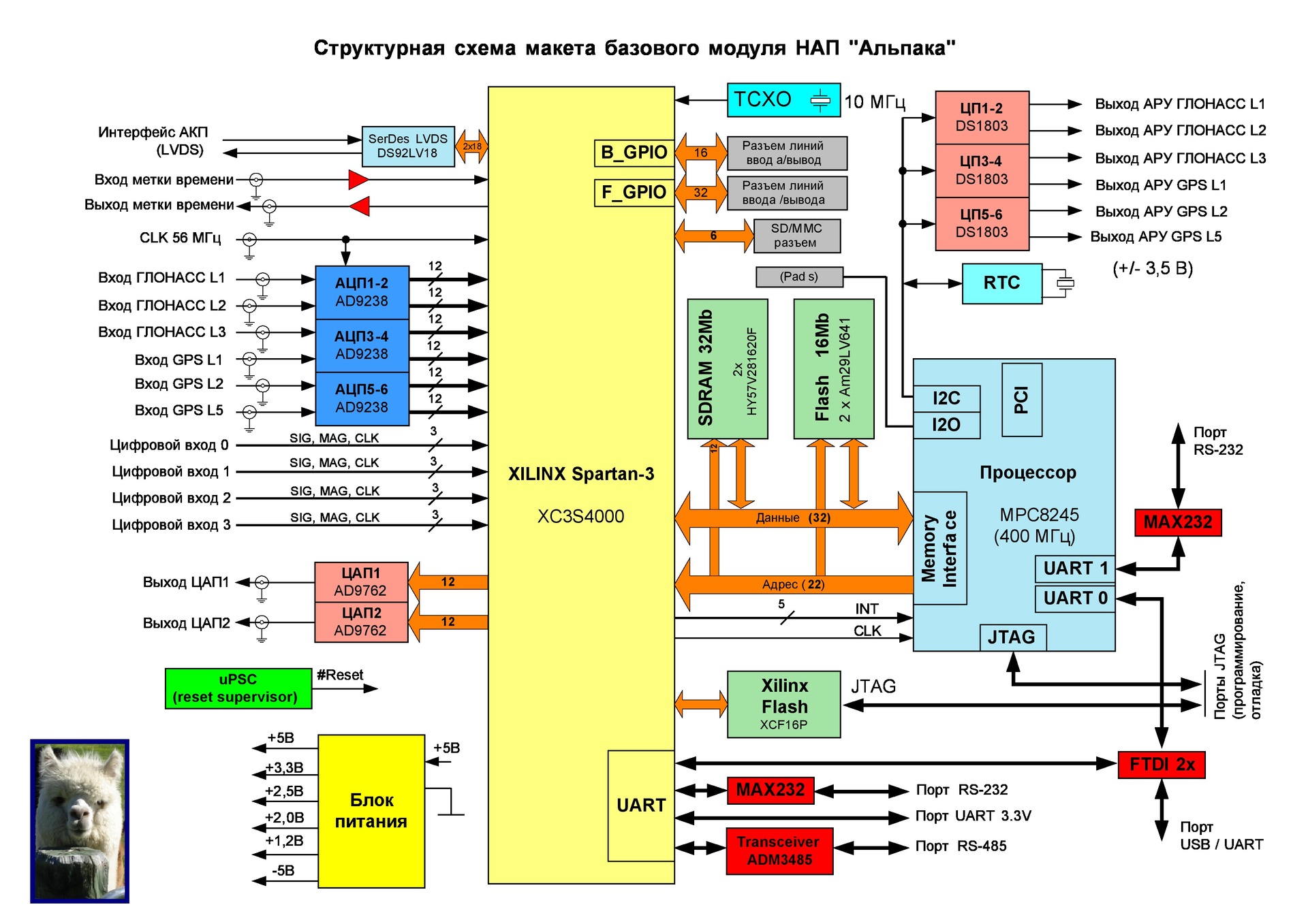
As the FPGA used was Xilinx Spartan 3, as the processor giant in the form of PowerPC MPC8245. Left plenty of time to transfer s architecture toolchains easy, finding drivers that exchange between the FPGA and processor and so on.
But suddenly the world has changed...
the
the Appearance of SoC that combines programmable logic and a processor system
The above-described pain is characteristic of small batch production and prototyping. For bundles of single FPGA + CPU is characterized by high cost, wild consumption and dimensions. And what's worse, the software portion of the product was unbearable. For each new combination had to rewrite a large part of the software.
As soon as the product could discourage the production of HAS and, the manufacturer has developed its own chip. In this chip combined all of the digital processing: ADC at an intermediate frequency, a parallel digital processing logic, a processor, interfaces. This scheme is built all modern navigation chips.
In the early 2010s, Xilinx and Altera have announced products that have solved half of our problems. Company Xilinx has started to produce chips of a series Zynq that combines programmable logic (FPGA) and processor system (dual-core ARM with a full set of peripherals).
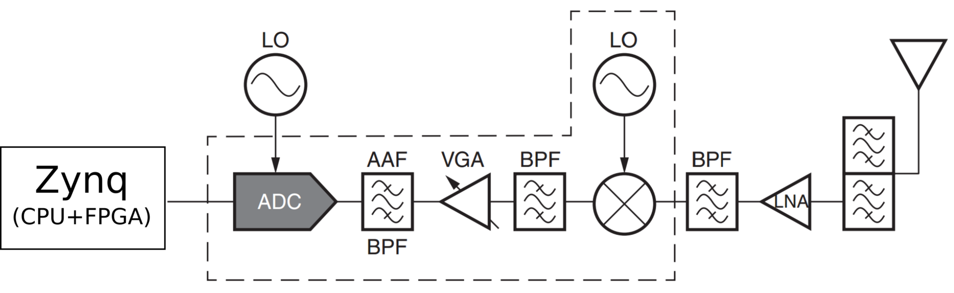
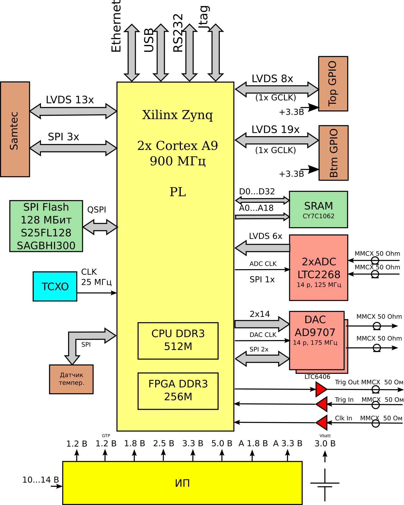
System-on-chip Zynq was a huge step forward. Greatly simplified the code that raised the rate of exchange between the processor system and programmable logic, simplified printed circuit Board. For example, a block diagram of one of our projects in 2013 and feel the difference:
And most importantly, unexpectedly was born a new quality: now our software runs on any Board with Zynq'ohms.
In the design cycle of an electronic device, the writing of algorithms and software, related research, working out is 80% of the time. If Java is cross-platform, the Zynq is a cross-board. Now we can shift the design Board to the customer, and focus on the main thing — software.
In addition, Xilinx has taken the issues architecture toolchains easy s, drivers, and other far from radio problems.
Five years after launch Zynq's there was an interesting phenomenon — commercial products based on programmable logic. An example is Piksi Multi or Tersus Precise. Yes, these receivers still consume more than the same built on ASIC. But the price was comparable! Little Zynq with a small amount of programmable logic can now be bought for $50! This increases the number of possible applications by orders of magnitude!
the
the future...
Considering the above, it becomes logical that the next step is to add the crystal ADCS and DACs. But the company Xilinx decided to make two steps forward.
Here a little more. Modern receivers or transmitters is two in the world. Digital and analog. For example, consider the receiver.
Analog world:
the
-
the
- antenna that converts the electromagnetic field into an electrical signal;
on the frontend, the function of which is to filter, amplify and lower the carrier frequency of the signal that it pulled digital processing.
The junction between the
Next comes the digital world, implemented a kind of computer.
Xilinx swung to the analog world!
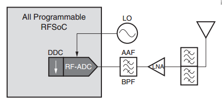
The ADC with an upper frequency of 4 GHz will go into digital processing directly on the carrier! DACs with the upper frequency to 6 GHz — throw out all the links to the power amplifier.
Such ADCS and DACs — 8 pieces! This closes the issues with mnogoatomnykh systems, which are every year becoming more urgent: MIMO, CRPA, Beamforming, orientation detection, etc.
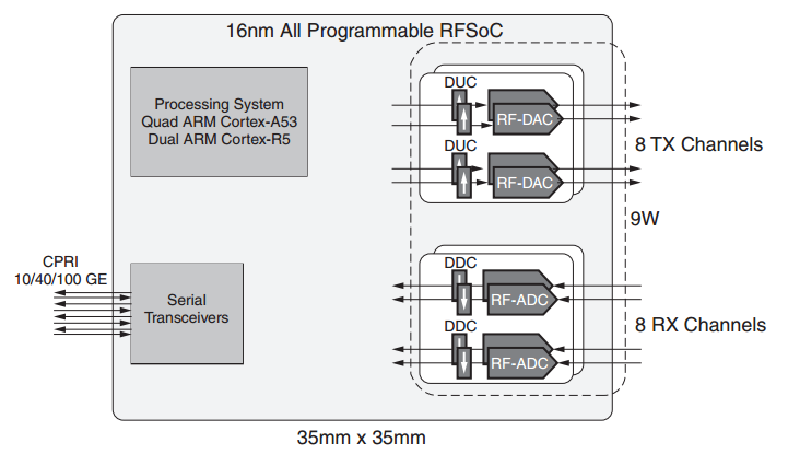
Analog-to-digital converters implemented on a single chip, which promises a high identity of their characteristics. They have high dynamic range of about 65 dB SFDR.
Thus, the analog part of the receiver boils down to the antenna, pre-filters, preamp. In the transmitter before the power amplifier and antenna. And one step of heterogenerous if your operational frequency above.
According to the statements of Xilinx, the use of the RFSoC can significantly improve the power consumption. In the version with 8 ADC and 8 DAC specifies a power consumption 27 watts.
As in the series of Zynq UltraScale, the processor system includes two processors for radio operators (a dual-core Cortex-R5) and custom applications (Quad-core Cortex-A53).
the
Summary
The announcement Xilinx'and reflects the General trend in electrical engineering is a course for unification and solutions all in one. Personally, it reminds me of the development of computers in the XX century. What are the implications for industry has brought the emergence of the same type of PC, what happened to the programmer and how the world has changed — recall is not required.
The main question now is — will you sell us this miracle? It remains to hope for a civilian version for the right price.


Комментарии
Отправить комментарий