Production of led display pilot batch of LaMetric
This article will interest those who are working on their own “hardware” project and faced a problem of manufacture of a pilot batch to test ideas in the real world. The story is based on my own experience in a startup Smart Atoms during the development of our product LaMetric – a clever led display with optional personalized settings.
In this article I want to pay attention to manufacturing and soldering circuit boards for the screen, and how to inexpensively enhance the quality of the soldering without wasting precious time.
the
Task
We started with the first prototype, which was implemented on the debugging tools in less than two weeks. After checking the idea, we had to make the first small pilot batch, for more thorough testing of all aspects of the product ranging from design to performance.
We were faced with stringent requirements on the screen and the housing size, some of them:
a) good color and clarity of display of each pixel;
b) the pixels should be perfectly square;
in) custom screen resolution;
g) the screen must be a part of the body like Nike+FuelBand;
Accordingly, led modules existing on the market does not suit us, “Makadi”, which was the first prototype is built, simply does not fit in the case.
We had to design and produce individual boards. The difficulties we met in this stage is soldering. We had to solder circuit boards with very small LEDs, the minimum size was 1.5 x 1.5 mm.
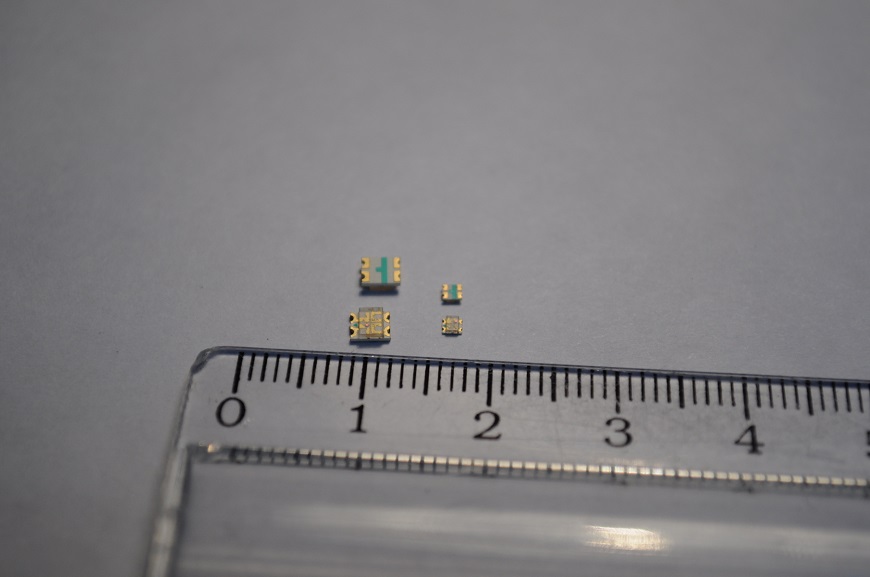
the LEDs in a tiny package
Manufacturers, with whom we had contact, not willing to want to mess with small batches, and if compromised, the issue price was great. Also not very pleasing to the stated terms and that the factories were far away from our city, and at an early stage of a startup it is very important to have everything at hand.
the
Solution
The first thing that came to mind to solder everything manually. Based on their own experience of soldering SMD components (surface mounted device), we knew that the risk of rejection will be large. Various kinds of defects (“snot”, not exactly sealed components and others) could lead to incorrect operation of the pilot screen and the party had a chance to fail.
Board defect “snot”
Therefore, instead of manual soldering, we decided to use surface mount technology printed circuit boards (surface mount technology).
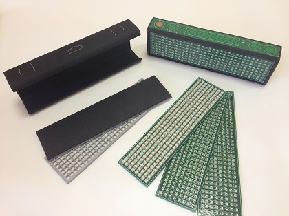
Designed Board, we started to look for the manufacturer's small batch four-layer circuit Board and the stencil. A stencil is a piece of sheet metal of stainless steel, which cut the hole (aperture) in those places where the solder paste needs to get on the contact pad of the mounted components. Also the stencil is stretched on the four sides on the frame to have less distortion in the plane. Search in the local market of comforting results are not shown. The first is price, second is time.
Ordered all Chinese service – Itead Studio. More details about the service can be found at article. The stencil was designed so that it contained several types of boards. You can safely place any number of boards within the dimensions of the stencil or to place upper and lower layers of circuit boards, it's “mirror”. After 7 days the order was ready. Shipping took 4 days. Regarding the quality issues have arisen. Everything was done on time.

Further, it was necessary to apply a solder paste to the Board. You will need four hands and a spatula. The extra area on the stencil to seal with tape. Carefully position the stencil and pressed it to the Board, further enhanced movements, with a spatula, apply the solder paste on the stencil. The result is cost with the optimal dosage of paste on each pad of the SMD component.
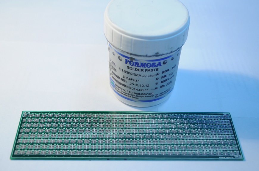
Board after solder paste application
The next step is to install the components. Components can be placed:
-
the
- with the help of forceps; the
- with a special “positioner installation of SMD components”; the
- with the help of “installation machine SMD-components.”
The easiest and best option for us is the first. The main thing is patience, good lighting, a “keen eye” and the presence of a magnifying glass.
We were also able to try the latter two options. The option arm is not very different from the tweezers. Option from the installation machine is not advisable to use in small batches.
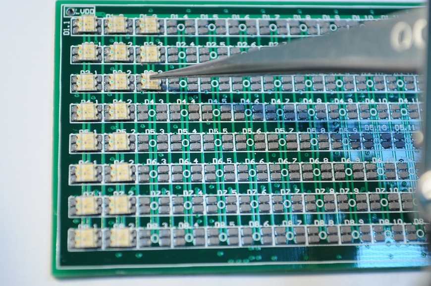
setting the LEDs with tweezers
The finish procedure, it is actually pike.
Options:
hot air soldering stations.
Exhibited a temperature of about 250-300 degrees. The main thing is not to overheat the SMD components. Gently, in a circular motion directed the nozzle of the hair dryer component. (time 10-15sec., the distance of 3-7cm.) If the component is installed not exactly, then under the action of surface tension will be self-positioning. Our recommendation is to first practice on a test samples, to deal with the temperature and strength of air supply, and then start the soldering.
using the furnace for soldering SMD components.
This method is used in automated production. In our city there is a small factory for the production of led lamps, where we found oven. The oven looks like a tube with different temperature areas. This tube is mounted a conveyor which with adjustable speed of the Board passing through each temperature region. Unlike the previous embodiment, the soldering process is much easier.
The quality of the soldering in both cases are identical.

circuit Board with soldered LEDs
The chronology we have tried to put in the video:
the Process of soldering circuit boards
the
Conclusion
This process has helped us to make a trial batch quickly and without errors. Just a few days we were testing the product on real users and real conditions.

a Pilot batch of the devices in “combat”
It was important for us to know all the intricacies of the process to understand all the nuances and to avoid mistakes when you start mass production. We highly recommend “hardware” start-UPS understand the process and solve any potential problems at the stage of a pilot batch.
In the next article I plan to discuss the technology of 3D printing, which we used for the housings.


Комментарии
Отправить комментарий